- testing
- morphology observation
- microstructure analysis
- surface element analysis
- surface foreign body
- component analysis
- mechanical property test
- thermal analysis
- welding qualification
- ct scan
- nondestructive testing
- cross section analysis
- coating thickness
- flame retardant test
- abration test
- coating quality inspection
optical microscopic morphology observation and measurement
| tin whisker | electron microscopy |
| surface roughness | intermetallic compounds |
| optical microscopic |
project introduction:
the optical microscope uses the zoom lens imaging principle to magnify the human eye cannot distinguish tiny objects to the size of the human eye can distinguish which is mainly to increase small objects near the eye opening angle (objects with large visual angle forms lager image in the retina). ordinary light wavelength is 400 ~ 700 nm, the best resolution of the optical microscope is 0.2 um, the resolution of the human eye is 0.2 mm, so the highest magnification microscope is usually 1000 x. the general optical microscope objective lens with multiple can be replaced, so observers can change the magnification as required. because of using visible light as light source, optical microscope for color recognition is very sensitive and accurate, not only can observe the sample surface structure but also can observe a certain range below the surface of the tissue.
applications:
optical microscope with easy operation, intuitive, and check efficiency characteristics, is suitable for surface observation and measurement. it can not only identify and analyze a variety of metals, alloys, non-metallic products, surface defects and integrated circuits, printed circuit boards, wires, fibers, surface coating and other surface phenomena checks, but can also be widely used in electronic, chemical industry and instrument material observation of opaque and transparent material.
visual inspection
purposes:
each industry pays more and more attention to the appearance issue and is stricter with product manufacturing process. products appearance rating largely reflects the quality of products. by using optical amplifier assist device check product appearance, assembly, surface defects such as cracks, holes and poor welding, test production line process, the quality of the printed circuit board and weld defects of circuit components etc; to help monitor the production process, take timely corrective action on test results; to provide guidance for the operation of the production process and product quality assurance; to ensure the products meet the shape, fit and functional requirements in the final use environment.
applications:
according to the using characteristic of parts, acceptance criteria generally include three conditions: ideal condition, acceptance condition, reject condition. mainly used in tooling fixture, metal parts, electronic products assembly, abnormal deviation, welding abnormal inspection, detects inspection of pcb/pcba lines, prevent welding, holes, parts alignment and text graphics.
test flow:
confirm the sample type→confirm the inspection specification→put the sample under the optical microscope and observe the phenomenon→result evaluation
reference standard:
ipc-6012,ipc-a-610 ,ipc-a-600
typical test images:
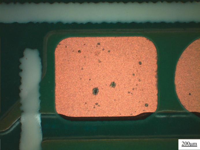
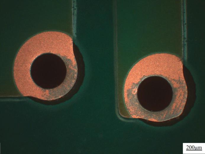
 |
 |
| foreign body on the surface of welding plate | foreign body on the surface of through hole |
size measurement
purposes:
measurement is the basis of the measure of material quality, comparing the physical quantity with the standard unit quantity, checking whether the dimensions/internal wiring conform to the requirements of the relevant standards and drawings. the size of the abnormal image artifacts can be stored for finding the cause and helping quick access to the actual size, product quality inspection and precise process control.
applications:
compared to traditional manual measurements and mechanical measurement, optical measurement size has high-precision (generally to 0.01mm), high speed (about 100 ms), objective, reliability, high repeatability, non-contact, no damage. it is mainly used in machinery, tools prototypes, small and medium-sized machinery, gears, cams, worm and other measurements, electronic components in electronic industry, inside and outside size of products (length, width, thickness, inner diameter and outer diameter), hole spacing, height and depth of the hole diameter measurement, the connector pin spacing, detection of coplanar degree, etc.
test flow:
confirm the sample type→confirm the inspection specification→select test position→
make sections (if necessary)→put the samples under the optical microscope to observe and take pictures→results output
reference standard:
ipc-6012,ipc-a-610 ,ipc-a-600
typical test images:
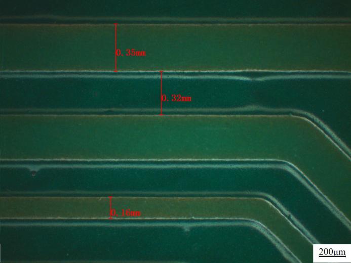
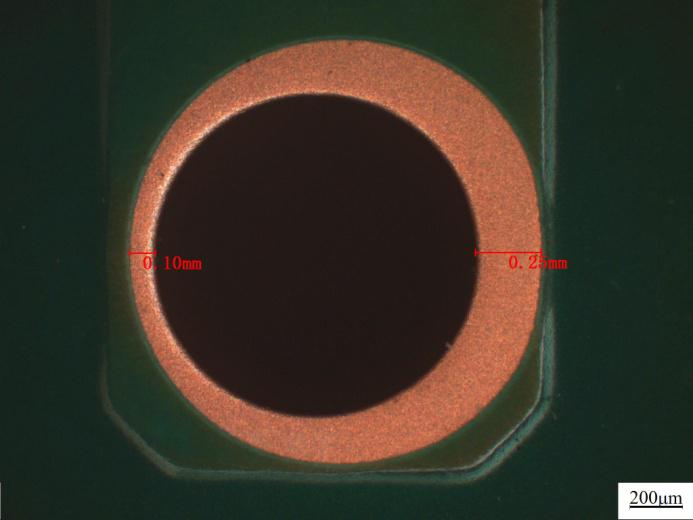
 |
 |
| line width / line distance measurement | hole wall thickness measurement |
- learn more
- qualification and honor
- contact us
- contact us
mtt shenzhen
tel: 400-850-4050
fax: 0755-2782 1672
email: marketing@mttlab.com
mtt suzhou
tel: 400-118-1002
fax: 0512-6275 9537
email: marketing@mttlab.com
mtt shanghai
tel: 400-118-1002
email: marketing@mttlab.com
mtt dongguan
tel: 400-116-1002
email:marketing@mttlab.com
