- testing
- morphology observation
- microstructure analysis
- surface element analysis
- surface foreign body
- component analysis
- mechanical property test
- thermal analysis
- welding qualification
- ct scan
- nondestructive testing
- cross section analysis
- coating thickness
- flame retardant test
- abration test
- coating quality inspection
x-ray energy spectrum analysis (eds)
| eds | fib |
| aes | xps |
| d-sims | tof-sims |
background:
in recent years, with the increasing complexity of the circuit design of electronic equipment, lead-free solders have become increasingly stringent, which urge that the study and application of chemistry nickel gold have been paid more and more attention, and new development has been achieved on it.
as the carrier of the various electronic components and the hub of the circuit signal transmission, pcb has become the most important and critical part of electronic information products. its quality and reliability level decide the quality and reliability of the whole equipment. but because of the cost and technology, a large number of failures have appeared in the production and application. for these failures, we need to use some failure analysis technique, to make the quality and reliability of pcb be ensured at the time of production.
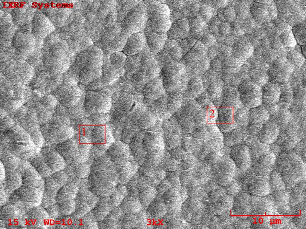
in the analysis of pcb, eds can be used to analyze the surface composition, such as the analysis of surface contaminant elements of the weldability poor pad and pin. quantitative analysis of eds has limited accuracy, less than 0.1% of the content is hard to be detected. with the use of sem and eds, we can obtain the surface morphology and composition at the same time , that is the reason of its wide use.
application range:
pcb, pcba, fpc, etc.
tested flow:
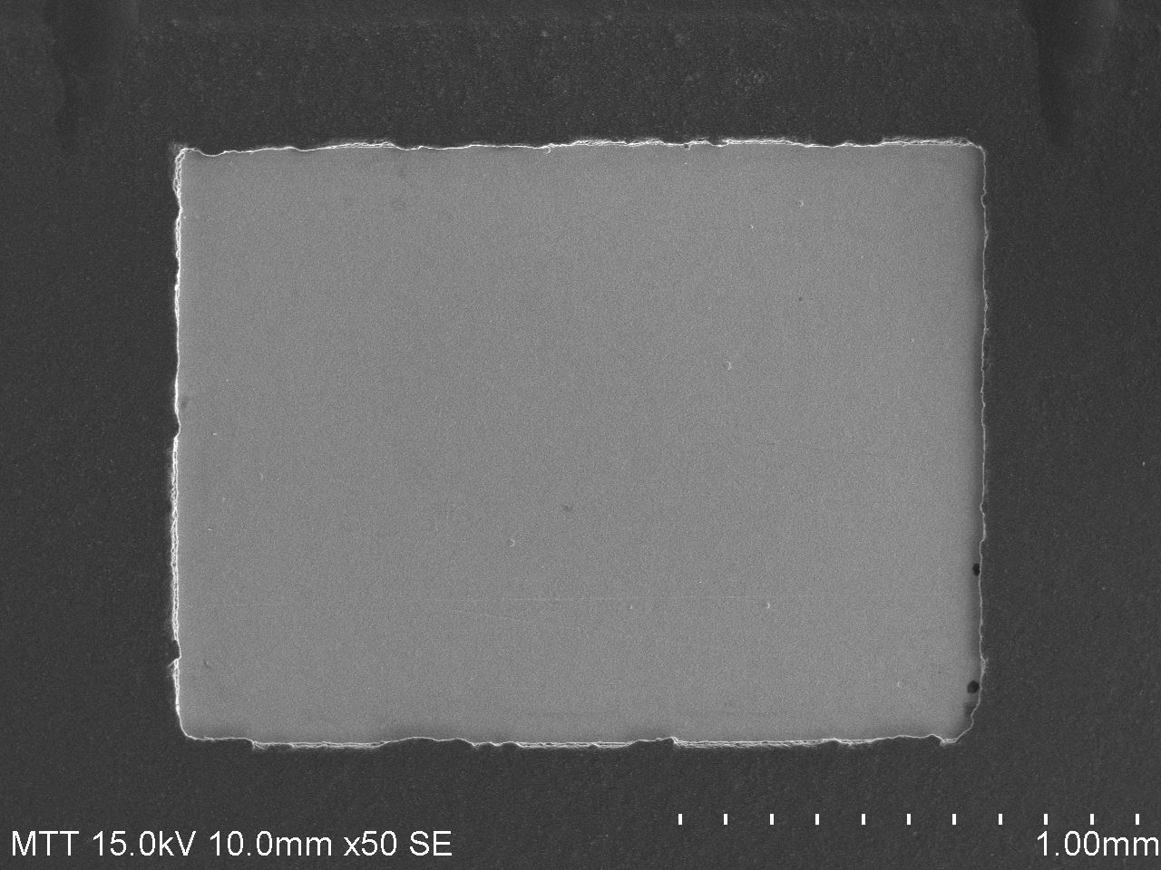
after sputtering pt on surface, the tested samples will be put into sem vacuum chamber to observe and detect the type and content of the surface elements by eds.
sample required:
the solid samples of non-magnetic or weakly magnetic, not easily deliquescence and no volatile, less than 8cm*8cm*2cm.
reference standard:
gb/t 17359-2012 microbeam analysis-quantitative analysis using energy dispersive spectrometry
typical pictures:
 |
|
| the test photos of pcb pad | |
 |
 |
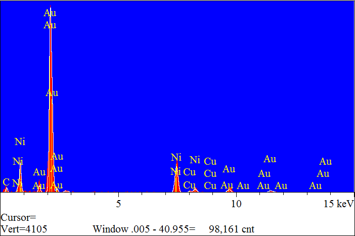
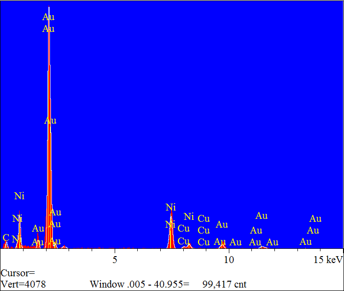
| the spectrums of components analysis | |
the test results of components analysis(wt.%)
| spectrum | c | ni | cu | au | total |
| 1 | 1.57 | 25.11 | 1.91 | 71.41 | 100 |
| 2 | 1.68 | 23.71 | 2.10 | 72.51 | 100 |
- learn more
- qualification and honor
- contact us
- contact us
mtt shenzhen
tel: 400-850-4050
fax: 0755-2782 1672
email: marketing@mttlab.com
mtt suzhou
tel: 400-118-1002
fax: 0512-6275 9537
email: marketing@mttlab.com
mtt shanghai
tel: 400-118-1002
email: marketing@mttlab.com
mtt dongguan
tel: 400-116-1002
email:marketing@mttlab.com

