- testing
- morphology observation
- microstructure analysis
- surface element analysis
- surface foreign body
- component analysis
- mechanical property test
- thermal analysis
- welding qualification
- ct scan
- nondestructive testing
- cross section analysis
- coating thickness
- flame retardant test
- abration test
- coating quality inspection
focused ion beam (fib)
| eds | fib |
| aes | xps |
| d-sims | tof-sims |
1.focused ion beam
focused ion beam (fib)use electricity lens which focus ion beam into a very small size to bombardment material surface,realize the stripping, deposition, injection, cutting and modification. with the development of nanotechnology,nanoscale manufacturing industry development is fast, nanofabrication is the hard core of nanoscale manufacturing, and fib is one of the representative methods. in recent years, fib uses high-duty ion beam to realizenano manufacture, by the help of sem in high magnification, has been the main way of nanoanalysis and manufacture, which is using in semiconductor integrated circuit modification, ion injection, cutting and malfunction analysis.
2.what can fib do for customers in product quality?
(1)if mistakes are found in micro etched circuit production, fib can cut or break the originalcircuit, make metal spraying in micro area, connect with other circuit to realize the modification which precision is about 5nm.
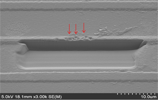
(2)micro or nano scale defects in the surface of product, for example, foreign body, corrosion, oxidation. fib can cut it in accurate position, make cross profile in defect position, and all these are convenient for us to observe the interface of defects and base material by using sem.
(3)for micro scale samples which have thin film by surface treatment, it needs to observe the thin film’s structure, combined degree. at that time, we can use fib to cut samples,then observe it by sem.
3.announcements in fib
(1)samples size 5×5×1cm, too big samples are unacceptable.
(2)electric conduction is necessary, if the samples are non-conducting, they must be able to spray god.
(3)50 um is the limit of cutting depth.
4.application examples
(1)cross profile of micro defects

(2)pcb crack position, using ion imaging to check the phase of copper foil.

- learn more
- qualification and honor
- contact us
- contact us
mtt shenzhen
tel: 400-850-4050
fax: 0755-2782 1672
email: marketing@mttlab.com
mtt suzhou
tel: 400-118-1002
fax: 0512-6275 9537
email: marketing@mttlab.com
mtt shanghai
tel: 400-118-1002
email: marketing@mttlab.com
mtt dongguan
tel: 400-116-1002
email:marketing@mttlab.com
